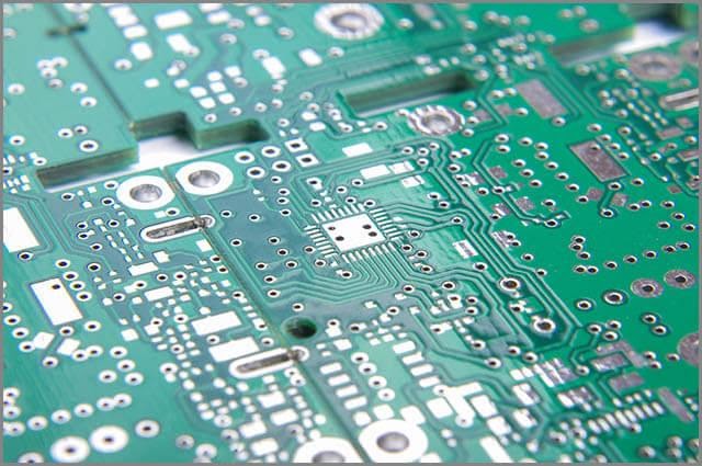
PCB boards are all around us in every gadget we use. Be it the smartphone or a simple calculator; their function depends on the performance of PCBs.
Do you know what the PCB circuit boards made of are?
PCB vs PCBA-What is the differences?
So, what is it that makes circuit boards so unique?
What makes one circuit board better than the other?
What does a circuit board consist of?
We have prepared this helpful guide,You can also get a picture of how a manufacturer produces them. Let’s begin by taking a look at what are the circuit boards made of.
Then, we will take a look at how you can make your circuit boards.
1. Custom PCB
1.1: What are the PCB prototype board or PCB Circuit Boards Made Of
Circuit boards are also known as printed circuit board or PCBs.Most of the PCBs are formed by combining two or more layers depending upon the complexity and nature of the device they will be used in.
PCBs use a variety of materials for their composition. One layer can be made from fibreglass or resin derived from paper. Apart from that other material such as copper, solder mask, and silkscreen layers are also used.
1.2: What Materials are Printed Circuit Board Made Of
PCB is generally made from four layers of material which are bonded together by heat, pressure and other methods. Four layers of a PCB are made of the substrate, copper, solder mask, and silkscreen.
The material encompassed by the printed circuit board includes:
• Copper: the copper gathers on the thick layer of foundation known as the substrate. Depending on the type of board and use, there can be one or two copper layers present.
• Silkscreen: the silkscreen performs the responsibility of making the printed circuit board readable to technology programmers by adding both numerical and letter indicators.
• Substrate: the substrate is commonly known as FR4, which is an acronym for Fire Retardant.
• Soldermask
1.3: Types of PCB
As briefed earlier, the PCB is a crucial component in different electronics. The type of printed circuit board includes;
Single-sided PCB
Double-sided printed circuit boards
Multilayer printed circuit boards.
Rigid printed circuit boards
Flex printed circuit boards.
Rigid-Flex printed circuit boards.
1.4: PCB components
Regardless of the idea behind creating any device, there must be components required for different circuits. The following are some essential components in any electronic product or device.
LED: LED is an acronym that means to cause a light-emitting diode. The led light-emitting diode allows current to pass through it; the current is only allowed to flow in one direction.
Resistors: Resistors perform very important functions by adjusting or controlling current, and in order to determine their value, they are colour-coded.
Battery: As a general function of a battery, it is responsible for providing energy. The battery is responsible for powering the circuit.
Transistor: The transistor plays a key role because it is responsible for the enhancement of charge.
Switch: The switch is used as a component for current control. The switch can be used to allow the current to enter or prevent current from entering.
Diode: A diode is a component that allows current to enter in only one direction. When the current flows in only one direction, the other channels are blocked.
Inductor: The inductor is responsible for the storage of charge.
2. What is PCB DESIGN?

2.1: PCB design basics
In discussing the basics of the PCB design, we require a background familiarity with the terminologies used. When referring to schematic capture, we talk about a program that permits the operator to make a schematic diagram of the component and other features. The schematic capture is just the representation of this in a graphical way. Other terminologies used include:
Gerber files: the Gerber files refer to those Computer-aided design files that are sent to the printed circuit board producers to build the PCB layer structure.
PCB layout tool: the program responsible for the layout of the PCB permits for the wiring connection structure to be applied on multiple layers and which after completion, allows the operator to generate the CAD files needed to make a printed circuit board.
2.2: PCB design steps
Below are the essential steps noted in the designing of a printed circuit board.
Step 1: use of a software
It is the designing of a printed circuit board with the use of software; it involves the schematic representation of the circuit with the use of the software. Examples of layout software that can be used are computer-aided design (CAD) software, mutism software, and eagle software. Let us make use of the eagle software in this article and in doing so, we have; Open the software board designs>>>click on file menu>>>select new design>>>click on library menu>>>select from the drop-down menu ‘pick devices/symbol’>>>double click on a relevant comment>>>add the components and represent the circuit with proper connections.>>>enter the rating of each component>>>click text editor on the command toolbar>>>click on variages>>>close the window>>>after the appearance of a black screen, save as an image format.
Step 2: the generation of film
With the aid of the finalized circuit board diagram of the printed circuit board layout, the generation of the film occurs.
Step 3: Selection of raw materials
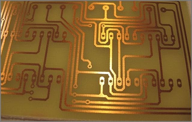
Less expensive printed circuit boards manufactured from paper phenolic bonded with copper foil are used in simple devices. The value of the copper-clad laminate is 0.059 thick with either single or double-sided board.
Step 4: Drilling holes
Hole in the PCB implemented using machine and drill bit. The first type of machine that can be used in drilling holes into the printed circuit board is the hand machine. This type of machine requires the effort of the operator to make holes into the board. The second type of machine is the automatic type called CNC machines. The programs they run provide the convenience of punching holes on printed circuit boards.
Step 5: fixing the image
In order to print the layouts on the PCB, laser printers are one of the best options in doing this. The process involved in this includes; placing a clean copper layer on the printer>>>storing on the computer the designed layout film>>>printing of the command received from the computer by the laser printer.
Step 6: Etching and Stripping
This stage uses a variety of chemicals to eliminate the useless copper attached to the printed circuit board.
Step 7: testing
After completing the above process, the board will be tested to ensure its functionality. In these recent days, many devices have been manufactured to aid the testing of the large volume of printed circuit boards.
2.3: PCB design software list
• PCB Artist
• Ultiboard
• Altium Designer 17
• SOLIDWORKS PCB
• DipTrace
• PCBWeb
• BSch3V
• XCircuit
• Gerbv
• KiCad EDA
• DesignSpark PCB
• Eagle PCBs
• CircuitMaker
• Pad2pad
• OrCAD
• ZenitPCB
• CircuitStudio
• PCB123
• CUSPICE
• FreePCB
The above list is the program used in the design of printed circuit boards.
2.3.1: PCB design software comparison
In looking at the comparison between printed circuit board designs, we would consider two software; this software is EAGLE CAD and DIPTrace. This two software are of course picked at random.
DipTrace features:
Capable of schematic captures with components linked to a library, the creation of patterns with the aid of a decent library editor, availability of perfect tutorial and support, high for smaller and simpler boards.
EAGLE CAD:
Electrical rule check, the schematic hierarchy for a design organisation, forward and backward annotation between schematic and printed circuit board.
2.3.2: best PCB design software
Out of the high number of PCB design software available these days, some plain ones are highly recognizable for their complete functionality.
• Readily Applicable Graphical Layout Editor (EAGLE): the eagle is a PCB design software that is user-friendly with moderate price. EAGLE has a wide range of proper function which includes: batch execution of script files, copper cladding, and more.
• Altium Designer
• DipTrace Lite
• DipTrace Starter
• Easy EDA
2.4: PCB design rules
There are some rules associated with the printed circuit board design that To use it effectively, and you need to remember it.
Width and Spacing: for the width and spacing, the parameters are usually denoted as “x/y rules” the X in this stands to represent the minimum of trace width while they in this represents the spacing, that is; the minimum trace spacing.
Thickness and size of the board: size and thickness can be set to suit the particular product. Many individuals use more boards on just a panel to conserve space and cost if mass production is to be done.
3. How To Make PCB Layout
3.1: PCB layout design
The printed circuit board layout design requires the technical know-how or professional skills that calls for the knowledge of the printed circuit board software, the printed circuit board computer-aided design system, and the skills or methods involved in the successful transfer of the basic circuit design to the final PCB.
3.2: PCB layout comparison
In the comparison of the printed circuit board, certain factors must be watched out for, and these include:
• The size of the board
• Layers available
• Power delivery network analysis
• 3D modelling
• Differential pair routing
3.3: PCB layout tutorial
This section will detail these steps:
Step 1: conversion of the schematic to a printed circuit board
Step 2: drag and drop the component
Step 3: sketching a custom outline
Step 4: copper area
Step 5: Routing
Step 6: Holes
Step 7: pictures and text
Step 8: photo view
4. PCB Reverse Engineering Software
In cases where the schematic may not be available, the data created from the printed circuit board reverse engineering can be used to produce replacement parts, or it can also give hints in repairing parts that already existed.
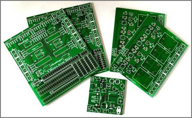
5. Custom Made Circuit Boards
We know that PCBs are complex elements and it can get a bit difficult for hobbyists to design themselves a working circuit. The first thing that you will need is reliable software with which you can create the blueprint of your PCB.
Then you can use many PCB design solutions such as Eagle from Cadsoft Computer which does an excellent job of designing your PCB.
Prepare Schematic View
You have to prepare the schematic view to create your custom PCB. Access the component library that is present in your design software and places them onto the canvas. Now you have to connect the pins along with the lines that symbolize electrical connections in the software.
The same part number may confuse you a bit as you will find several options to choose from. The different packages can include the surface-mounted chip or a Dual-in-line package (DIP). If you are a hobbyist or doing a DIY project, then it makes sense to go for significant and noticeable system-in-packages (SIP) or DIPs.
You can find them quickly, and hobby outlets and are far friendly when it comes to soldering them compared to surface mounted devices, which are reserved for commercial applications.
The different packaging options can appear to be similar in the schematic view. However, things will start to appear different when you switch to layout view to begin your designing.
You will need to provide the necessary ground and power signals apart from placing your interconnections and components; you can use the components such as GND, VDD and VCC found in the Eagle library for the job.
You shouldn’t also forget to integrate the connectors on the board so that the ground and power can be employed. At this stage, you will also have to any exterior device you want such as a potentiometer or LEDs.
Your design now needs to go through electrical rule check or ERC after you have put everything in place. The test is crucial to ensure that there is no error present which will hamper the functionality of your circuit board.
Some of the common issues that you mace are wires which appear to be connected but are not in reality. You can check for little dots in your Eagle software which represent the connection intersections of the wires.
Other problems may include ground and power signals that you forgot to connect. So you should remember is that the automated tests won’t tell you if your board is going to carry out the desired action, but it can always validate the electrical properties of your design.
Access Board Layout View
After you have done everything that you need to do in the schematic view, you have to move over to activate the board layout view. Then you have made the switch, and you will find the components spread randomly in your Eagle software. You will also see that the wires directly hook to the pins.
To make the picture a bit less messy, move the components until they make meaning. For example, you can move the connectors to the edges so that things make sense. You still have much work to do to produce the circuit board. So you have to dedicate signals to the layers but remember that the different layers present in the same sheet should not touch each other.
The professional version of the Eagle solution comes with an auto-layout feature that can route the signals with a single click. However, for users of the standard text, you have to take things in your own hands. You may also find a design solution from your PCB manufacturer to take care of this step.
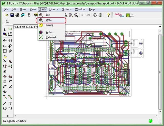
After you have laid down the signals, the time has come to run the DRC or the design check. The check ensures that holes drilled too close to a signal line. It also notifies you if the traces are not at an optimum distance from each other or the edge of the board.
You can customise the rules, and sometimes your PCB vendor will offer a file that can be integrated with Eagle solution with specified DRC values. Then you can move ahead and upload your design files if your project passes the DRC.
You should utilize a particular layer to add silkscreen lettering to the top. The printing will help you know which component fits whereby presenting part numbers and outlines. That enables you to avoid mistakes like placing a 100K resistor instead of a 1K one.
A Gerber file reveals the language of PCB design, and the 3each board can have any data associated with them. You will have separate data for specifications of the solder pads and different files for each layer. The drill files also carry the specifications of the drilling.
You can then upload the design with your manufacturer who can use another program to present the final look of the layers, and you can also find out if the components are the right size to fit the holes.
With this, you have come to the end of creating a custom circuit board using design software. In the next chapter, we will explore how a manufacturer produces PCBs.
6. How are Circuit Boards Made
We are going to discuss the PCB manufacturing process in brief just for you.
1. Making the Substrate
2. The Copper Layers
Next, you have to print the pattern of the circuit on the PCB.
3. The Final Solder Mask
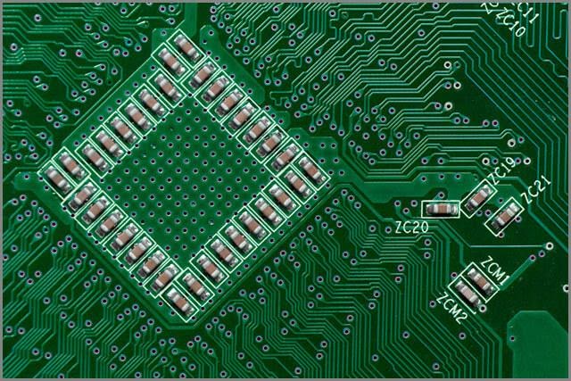
The metals which remain exposed on the circuit board have a chance to get damaged. A nature of copper is to corrode, which will render your PCB useless. You can adequately protect the copper plating and other components of the PCB by adding an extra protective layer on top.
Generally, manufacturers use gold, nickel or tin-lead to plate specific vulnerable parts of the PCB. To top it all, the manufacturer provides another layer on top called the solder mask.
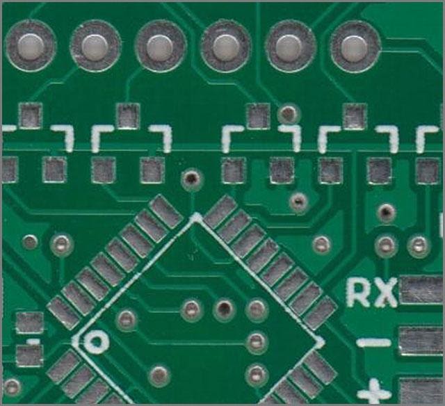
The green colour that you see in PCBs is due to the application of the solder mask layer; the solder mask also has some other functions apart from covering and protecting all the metal parts that don’t need to form a connection with anything, the layer of solder mask also ensures that current flows to the right places following absolute paths.
Sometimes you may also find a layer of silkscreen on top of the solder mask which is used to carve labels on necessary parts.
After everything is done, the manufacturer will trim and shed off any extra material or unnecessary parts that are not required in your PCB.
7. Conclusion
The best for just you.We have given you the gist, and we can only hope you liked and benefitted from this. You wouldn’t want to hesitate on this any longer, we are right behind you, and just a call will do! Contact us today and secure your interest in high-quality products.