Overcrowding your PCB and not working within the space you have is very costly. The size and design complexity are huge factors that directly affect PCB costs. Overcrowded PCB designs also cause PCB shorts and malfunctions. Managing your board to work within the set space parameters saves and earns you time and money.
Electric Shorts
Common Soldering Problems
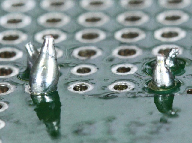
Constant electric shorts are a common occurrence with high-frequency designs. Unfortunately, shorts happen even with well -designed PCBs, and as long as you have a high-frequency design, soldier bridge shorts are here to stay. High-frequency designs are inevitable with more demands on them by PCBs.
When you have to decrease pad size and the distance in between, you have more solder paste, albeit in a much smaller space. The paste overspills out of the set stencil areas and ends up creating solder paste bridges to adjacent pads. You avoid the bridges by having some space in between that holds the spill from the adjacent pads.
Manufacture
PCB Basics
Stencil problems increase solder-bridging risks, especially in the squeezed component. You must ensure you have cushioning space to enable your PCB design to forestall solder bridges. If the cushioning space is not there, then soldier bridges will definitely form and cause shorting.
Machine accuracy puts a limit on the density allowed in the board design, and if the machine accuracy is high, you get more flexibility in the constituent materials. The height of the component is a problem only if the Pick and Place find it hard to access the location, especially adjacent to a taller component. An example is resistors adjacent to headers.
Inspecting, reworking, and Repairing
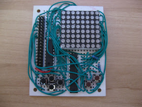
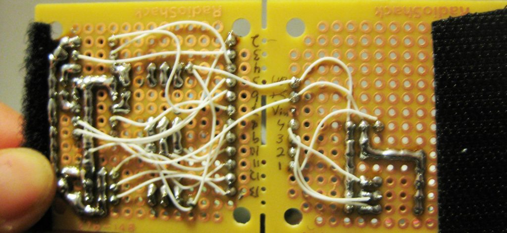
How do I connect components when using a circuit board with pads but no traces?
Post-manufacture, the complexities of a high-profile design still exist. Inspecting becomes a challenge, as components’ edges are partly visible only when close-knit unlike in high profile designs. Detecting the problem in a high profile design is not the issue. When you compact the components close to each other, you find other processes, which slow, or raise errors. To get to the problematic component, you must remove the different components to access the compound you desire. The component that needs fixing will remelt the paste and cause slippage.Since there is little room for heat dissipation, you need to include a heat shield for the adjacent components.
Spacing Requirements

Understanding Solder Bridge Shorts: Bake Your Cookie and Eat It Too
Operational requirements demand prioritization on component spacing. There are spacing specifications and the most common is IPC-D-279, section 3.3.9. The minute you have varied packaging and component types, these specifications are not enough to supply enough guidelines.
The stipulations guiding component spacing bank on the board’s function, the surroundings and operation specifics. The isolation needs premise on the RFI, EMC or Voltage, so you must consider these, or else you will end up causing damage to your product. You might come across handling stipulations that pin down edge spacing. At first, buffering appears like a simple way to reduce costs, but it might have dire repercussions on the board’s lifespan. During design, keeping track of component spacing and solder bridge shorting might seem like a headache, and it may be hard to multitask. The implications, however, are rewarding. They will ensure you get a quality product at in the end.
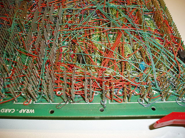
How to make traces on an universal PCB?